The computational power of AI hardware continues to increase at an extraordinary rate. To meet the world’s soaring demand for more AI compute, it’s not enough to just build new chips capable of more and more operations per second.
To make advanced AI accessible to everyone, AI hardware must deliver two critical things on top of being able to perform many computations in parallel:
- Programmability. AI hardware must accommodate the rapid pace of innovation. Today’s large-scale transformer models and diffusion models place different burdens on AI hardware than convolutional networks, for example, and tomorrow’s generative models will tax hardware in ways that can’t be predicted. This is why leaders like OpenAI’s Greg Brockman have highlighted the need to “build better chips that are optimized for not just today’s models, but to be really able to see where the models are going.”
This kind of programmability is possible with GPUs, but it is often not easy to achieve. Obtaining peak performance with a new model often requires hand-tuning kernels and other time-intensive compiler optimizations.
- Power efficiency. This is a crucial limitation of the GPU chip architecture. Each generation of GPUs consumes much more power than the last, with the latest hardware using more than 1,000W per chip. These chips are increasingly expensive to run and difficult to cool, not to mention an increasingly important part of the challenge of mitigating climate change.
GPUs offer tremendous computational power, of course, but they struggle to combine this with easy programmability and power efficiency. Compute, programmability, and efficiency will shape who benefits from AI. If tomorrow’s most useful AI tools only run on difficult to use, extremely energy intensive chips, those tools will be out of reach for most people.
Meet the Tensor Contraction Processor: A leap forward in AI hardware
To make high-performance AI computing sustainable and broadly accessible, FuriosaAI has developed a new chip architecture, the Tensor Contraction Processor (TCP), which addresses all three of the needs described above.
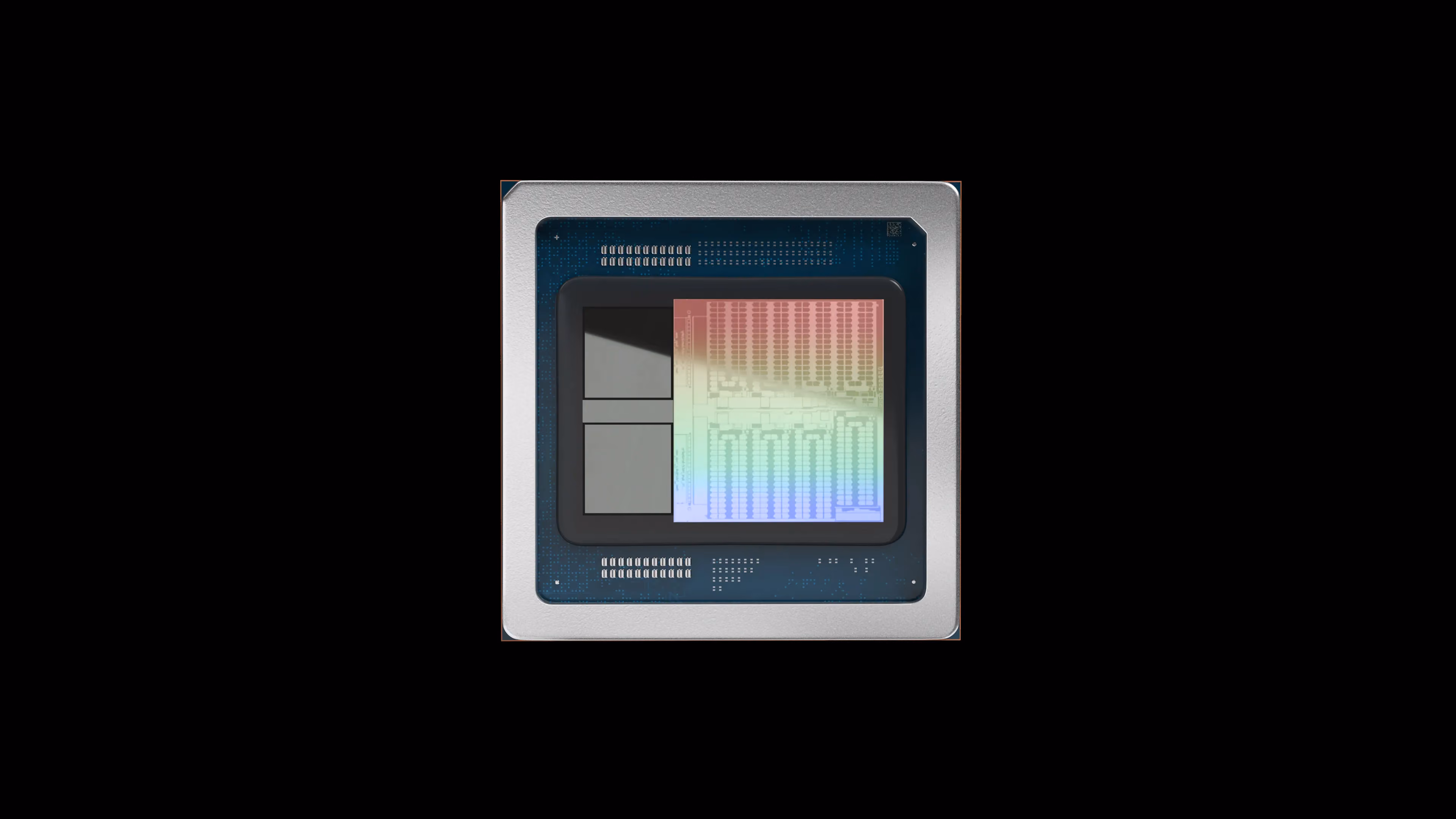
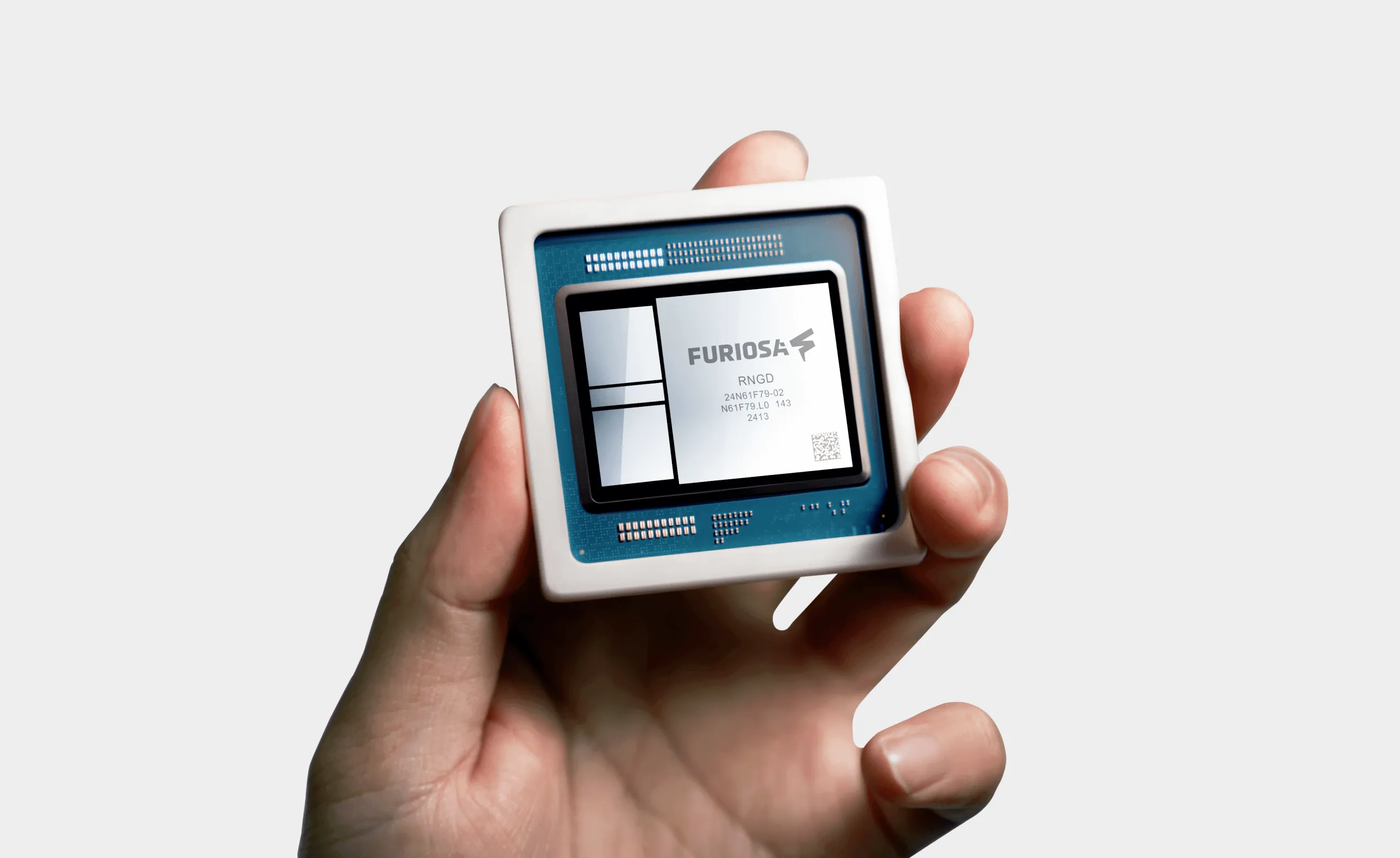
The TCP architecture is built around the core computation of AI, so it can manage data and memory much more efficiently than is possible with GPUs. This means our second-gen TCP chip, RNGD (pronounced "Renegade), delivers the computational power to run high-performance generative AI models like Llama 3, as well as significantly improved power efficiency.
It is also highly programmable, because we co-designed TCP in tandem with Furiosa’s advanced software stack, which includes a general compiler that can treat an entire model as a single fused operation. This makes it possible to deploy and optimize new models automatically, even when they use a novel architecture. This is something that is not possible with GPUs because they allocate resources dynamically, making it difficult to precisely predict performance.
In this blog post, we highlight TCP’s key architectural innovations. Additional technical details are available in our research paper, TCP: A Tensor Contraction Processor for AI Workloads, which was recently accepted by the International Symposium on Computer Architecture (ISCA), the leading forum for new ideas in silicon design.
We are currently testing the first production samples of RNGD, which uses the TCP architecture to run large language models and other generative AI applications.
RNGD will launch later this year. We believe it will be a turning point for the industry and pave the way for everyone to have access to the compute needed to run the most powerful, most useful AI technologies. You can learn more about RNGD in this blog post previewing the launch of the chip.
Matrix multiplication is not all you need
For all chip architectures (including CPUs, GPUs, and our TCP design) transferring data between DRAM and the chip’s processing elements uses much more energy (as much as 10,000 times more) than performing the computations themselves.
This means that, in order to implement AI algorithms efficiently, chips must minimize data movement by reusing data already stored in on-chip memory. If data can be divided into predictable, repeatable patterns or segments, it can often be used more than once (for example, by taking a single weight matrix and calculating the dot product with many different inputs).
Data reuse is particularly important with large language models and other generative AI because of the vast amounts of data involved. With models that are much too large to fit in on-chip memory, data reuse is essential to improving efficiency and overall performance.
To understand the most effective strategies to reuse data, it is important to look at how AI models organize data.
AI practitioners typically think of their data as matrices (data structured in just two dimensions) and computations as matrix multiplication. This is true in part, but not entirely. AI models mostly involve operations with tensors, which are the generalization of matrices to higher dimensions. (Nontechnical readers might find it useful to think of tensors as data structured as a 3D cube, but of course tensors can have more than three dimensions.)
The input to an AI model – such as an image, video, text passage, or audio clip – is organized into tensors. So are the model parameters and the intermediate layers, and often the output of the model as well. The attention mechanism in transformer networks are likewise operations performed on tensors (as are other operations like convolutions).
When we think of these calculations as matrix multiplications, it is only because an extra step is performed first to reshape or divide up the tensors. Matrix multiplication is one type of the more general tensor contraction operation.
Tensor contraction generalizes matrix multiplication, allowing for more complex and efficient data interactions that reduce the computational overhead by combining elements across multiple dimensions in a single operation. This not only leverages the inherent multidimensional nature of tensors for more extensive parallelism but also enhances data reuse across these operations.
When a tensor is flattened or broken into a 2D matrix, this parallelism is often destroyed. For example, the input to a language model might be a 3D tensor with different axes for batch size, sequence length, and features. Reshaping it into a 2D matrix might obscure the distinction between the different sequences and makes it much more difficult to exploit the fact that the data contains multiple sequences of text in parallel.
Working with AI data in its natural form
Furiosa’s Tensor Contraction Processor architecture is designed to address these limitations and maximize data reuse. In contrast to GPUs, the fundamental data structure for the TCP is the tensor and the fundamental operation it performs is tensor contraction. This means the TCP does not need to take the extra step of dividing tensors into 2D matrices before performing computations.


The example below shows simplified illustrations of Key and Value tensors, which are multidimensional data structures used in transformer models. Each tensor in this simplified example has separate dimensions for sequence length, input tokens, and the number of attention heads. The two tensors are each subdivided into smaller partitioned tensors and then transferred from DRAM into the SRAM of each processing element in the TCP chip. Reading data from DRAM consumes much more power than performing computations with the data, so the TCP architecture is designed to maximize reuse of data already stored in SRAM.

Once they are stored in each slice’s SRAM, the Key and Query partitioned tensors can be divided into one-dimensional vectors (without the need to divide them into two-dimensional matrices first). Each slice takes vectors from the Query partitioned tensor and “streams” them from SRAM into the Dot-Product Engine, where the computations take place. Data is also multicast from the SRAM of each slice to other slices, which enables greater data reuse without additional DRAM reads.
Note: The multicast data is delivered through the fetch network router, but that is not shown in this simplified illustration.
In the example above, we show how TCP architecture computes a common tensor contraction used in multi-headed attention: QK ᵀ. This computation is a core part of transformer models, where we find the dot product of the Query vector and all the Key vectors in order to generate a matrix of the attention scores between each pair of the input tokens.
QK ᵀ can also be expressed in einsum notation (a common way to concisely express tensor operations): It is hqd, hkd->hqk, where h stands for the number of heads, q and k stand for Query and Key tensors, and d stands for dimension size of each head. The contraction operates in parallel along the h axis, with contraction occurring on the d axis.
As shown in the graphic, both the Query and Key tensors are fetched from DRAM only once, then stored in SRAM and reused repeatedly for all QK ᵀ operations.

To further minimize data movement, the chip uses the output activation of a layer directly as the input activation of the next layer in on-chip memory – without any additional DRAM accesses.
A long-term roadmap for building a new chip architecture
We know the AI space is filled with both new and established companies making bold claims that can be hard to assess. That’s one of the reasons Furiosa has taken a methodical, long-term approach to building AI hardware.
After our three co-founders (engineers with decades of experience at Samsung, Qualcomm, and AMD) started our company in 2017, we first spent several years testing and validating the ideas that underlie the TCP architecture. When this underlying work was complete, we launched our first TCP-based Gen 1 Vision NPU in 2021 as a commercial product in partnership with Samsung and ASUS. This enabled us to get real-world feedback from customers and use it to later improve RNGD.
In 2022, Furiosa was the only AI silicon startup to submit results to the industry-standard MLPerf inference benchmark, showing that our Gen 1 Vision NPU outperformed NVIDIA’s A2 chip in vision tasks.
Having validated our TCP design with Gen 1, we designed RNGD to run the most demanding AI algorithms. We’re excited to launch RNGD later this year, with more TCP-based chips to follow.
Creating a hardware ecosystem to meet the demand for AI compute
As AI research advances and more applications enter production, hardware efficiency will matter more and more. Even with powerful techniques like model distillation, weight pruning, quantization, and weight sharing, the most capable AI models will continue to be computationally demanding.
Many hardware innovations will help the industry meet the demand for more capable AI processors. A few of the most important are new forms of high-bandwidth memory, PCIe 5.0, and 2.5D packaging. Each of these advances (and many others) will have a significant impact, but to create an era of truly abundant AI compute, we must start with the chip architecture itself.
With a new chip design focused specifically on tensor contractions, the industry will be able to leverage these other advances even more effectively. We look forward to launching Furiosa’s second-generation RNGD chip this year to begin this new chapter in AI hardware.
Sign up here to be notified first about RNGD availability and product updates.here to be notified first about RNGD availability and product updates.
Written by
Hanjoon Kim
Chief Technology Officer