High Bandwidth Memory 3 (HBM3) is, to use a technical term, a pain in the ASIC to implement.
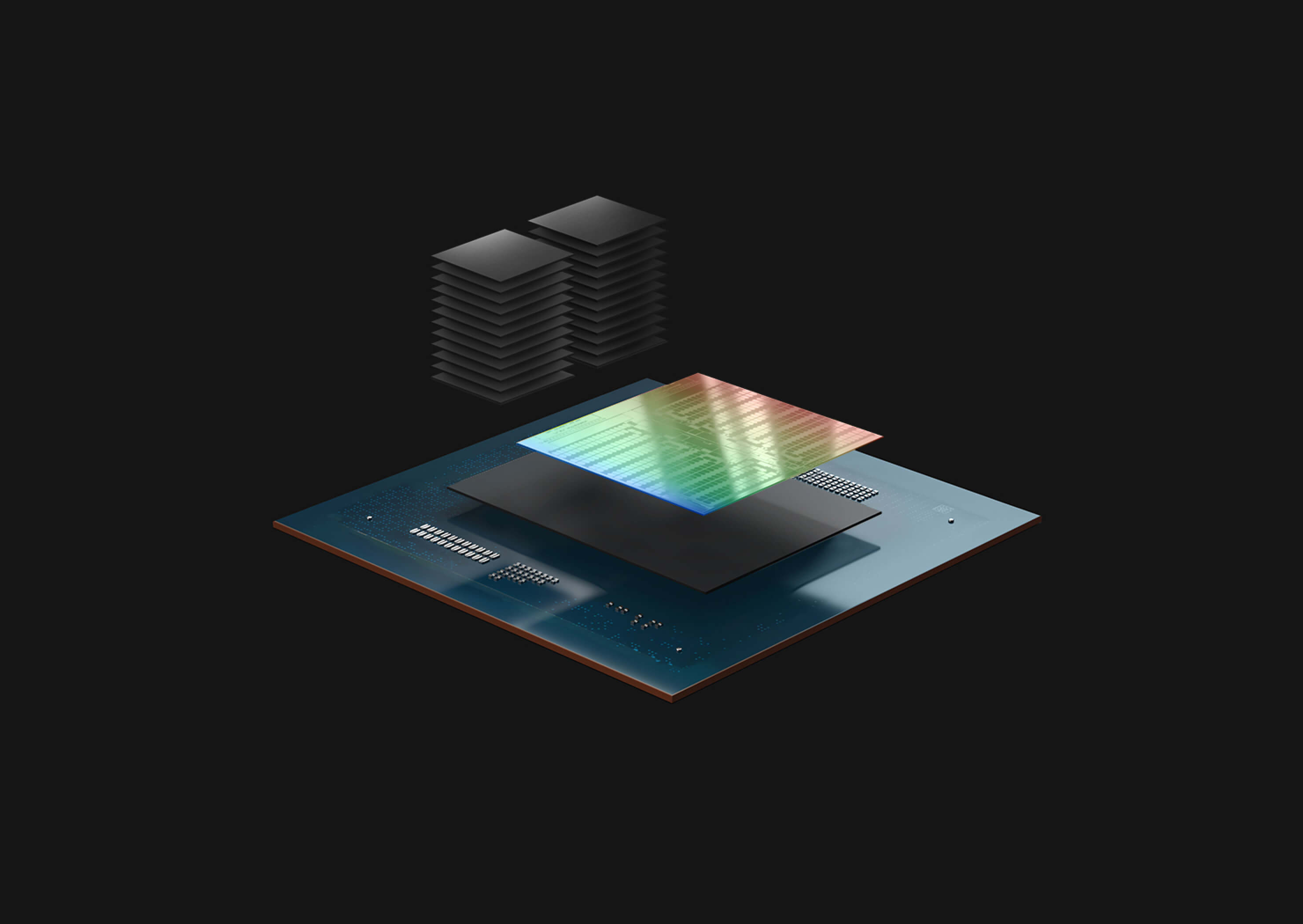
Unlike traditional GDDR memory, HBM3 uses a complex 2.5D packaging design and requires specialized interposers and advanced packaging techniques. Most importantly, HBM3 presents significant thermal management challenges, because the dense stacking makes it difficult to dissipate heat and, while HBM3 is energy efficient per bit transferred, its high bandwidth capabilities mean the overall power draw can be very high.
There is a reason few AI silicon companies use it, aside from the very largest chipmakers that have hundreds of engineers they can assign to address these challenges.
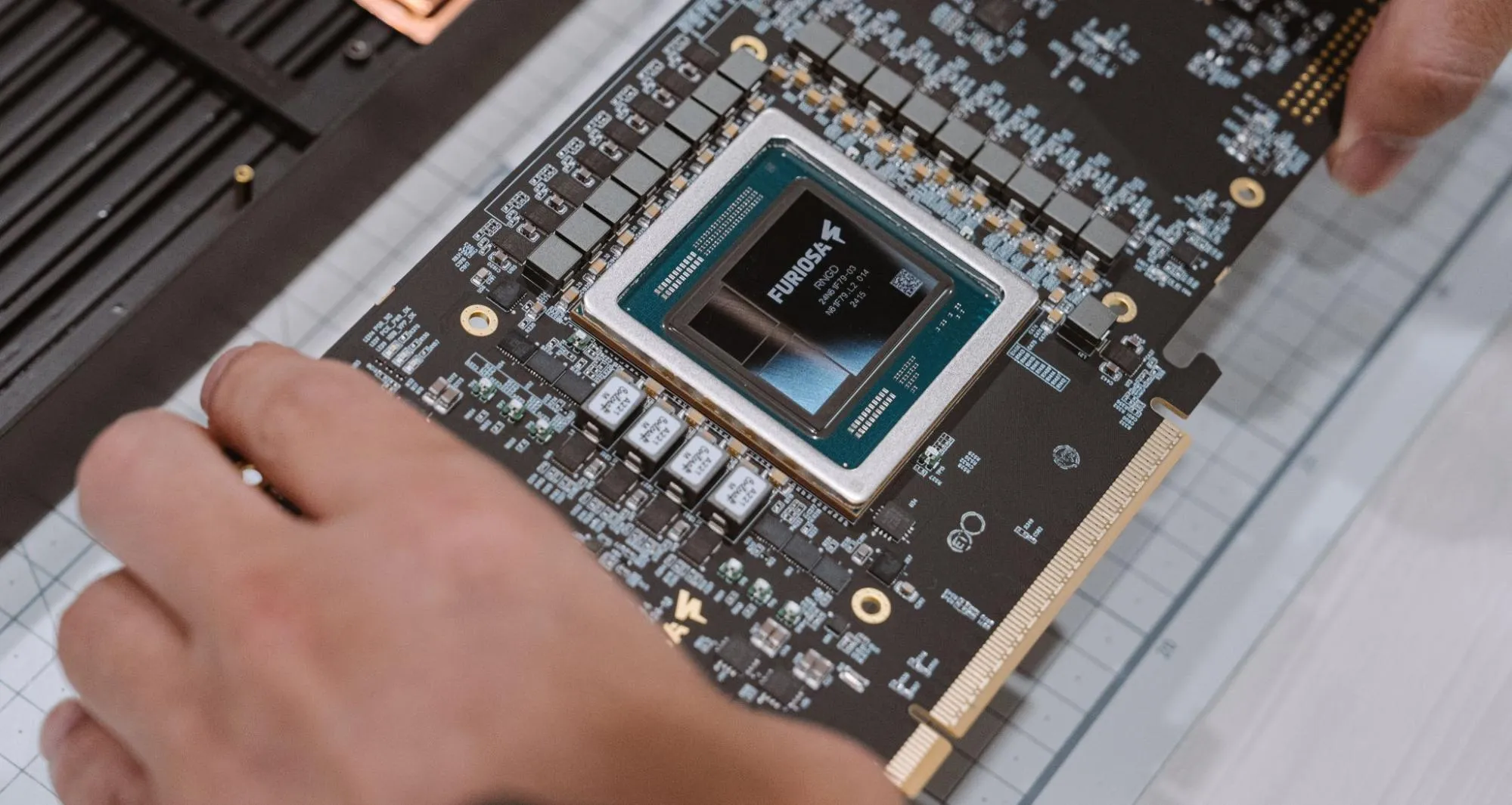
Nevertheless, HBM3 was the right choice for RNGD, FuriosaAI’s second-gen chip. RNGD (pronounced “Renegade”) is built specifically for inference with high performance LLMs and multimodal models. This means RNGD needs tremendous memory bandwidth that only HBM can provide.
Now that RNGD is in production and our early access partners have begun sampling the chip, Furiosa’s hardware engineering leads sat down together to discuss how we implemented HBM3 and what we’ve learned about building AI hardware that delivers the “trifecta” of performance, programmability, and power efficiency that the industry needs.
This roundtable features Furiosa CTO Hanjoon Kim, who has a background in both hardware and software engineering and previously worked for Samsung; VP of Hardware and Engineering Lead for Chip Packaging Sang Min Lee, who previously worked for Qualcomm as a Senior Staff Engineer; and Furiosa Engineering Lead for SoC Interfaces Chang Jae Park, who joined Furiosa after working as a Research Fellow and Senior Engineer at SK hynix and as a Principal Engineer at Samsung.
How critical was HBM3 in achieving our performance targets for RNGD? What specific benefits does HBM3 provide to enhance RNGD's capabilities?
Hanjoon Kim, Furiosa CTO: HBM3 is one of the key factors that most directly impacts the performance goals of RNGD, because the chip is designed for LLMs and multimodal models. Because these types of models are so big, memory bandwidth is a bottleneck.
In LLMs, every time a token is generated, all model parameters must be read from memory once, and since the size of the model parameters is large, the token generation speed is determined by memory bandwidth.
Additionally, HBM3 is important in terms of memory capacity. A larger memory capacity allows larger models to run on fewer chips, reducing the bottleneck impact of interconnections. It also allows for more key value cache storage, which increases the batch size that can be processed at once, thereby improving throughput. Therefore, high memory bandwidth and memory capacity of HBM3 are crucial from a performance perspective.
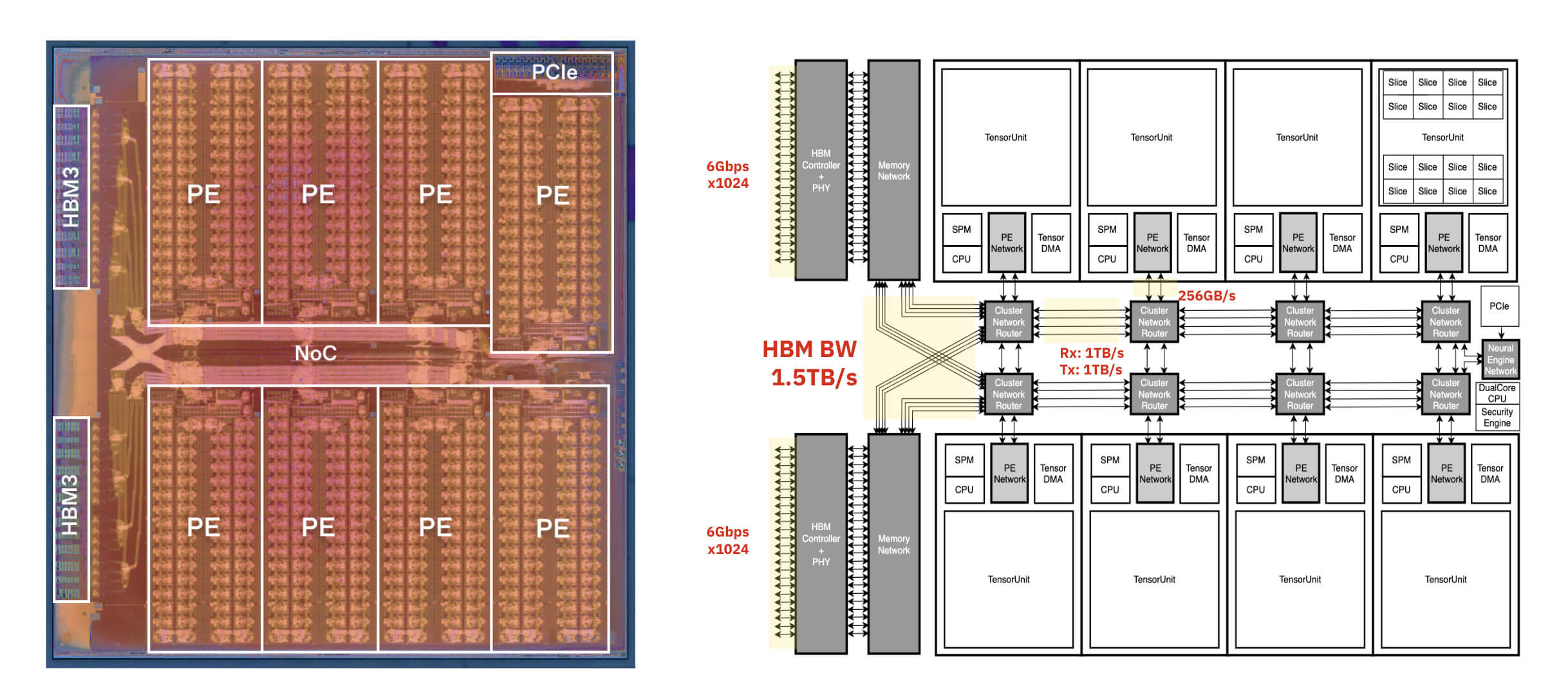
Furthermore, HBM3 is highly efficient in terms of energy consumption per bit transferred. The most energy-efficient method to provide memory bandwidth levels of around 1.5 TB/s is HBM3.
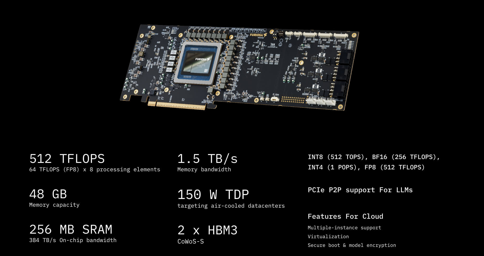
This is especially important for RNGD because the chip provides 1.5 TB/s of memory bandwidth and 48GB of memory capacity within a TDP of 180W. RNGD offers the highest levels of memory bandwidth and memory capacity per unit power among accelerators, and the biggest factor is the use of 12-layer HBM3.
Can you provide examples of key RNGD use cases that wouldn’t be feasible without the integration of HBM3?
Hanjoon: For the Llama 3.1 8B model with weights quantized to BF16, the size of the model parameters is approximately 16GB. Since 16GB needs to be read into the chip each time a token is generated, at a memory bandwidth of 1.5TB/s, it ideally takes 11ms, allowing a maximum output of 94 tokens per second. If GDDR is used with a memory bandwidth of 300GB/s, it would take about 5 times longer, thus limiting the maximum output to 19 tokens per second.
HBM3 is cutting-edge technology. What technical challenges did you anticipate when deciding to incorporate it into RNGD? How did these concerns influence the design process?
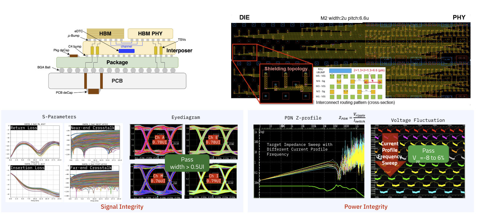
Chang Jae Park, Furiosa Engineering Lead for SoC Interfaces: As mentioned, HBM3 is a new technology that Furiosa hadn’t implemented before. Moreover, HBM is connected to the SoC via a silicon interposer that is packaged with HBM, so there's little room for observation, debugging or control once it's packaged. We had to be very careful at the design stage, especially for SI/PI at the package level.
Sang Min Lee, Head of Hardware and Engineering Lead for Chip Packaging: The decision to integrate HBM3 was a major factor in our decision to work with TSMC and GUC to build RNGD, since both these companies have an established track record with the technology.
Can you elaborate on the specific thermal management solutions implemented in RNGD to address the heat dissipation challenges of HBM3?
Sang Min: We created a thermal model including HBM, SoC, the interposer, and the package so that the model can represent the thermal coupling between HBM and SoC, and also it can model the thermal dissipation both to the chip top and to the chip bottom. We used this model to extensively simulate the thermal performance of the custom heat sink we have designed – even considering the server airflow.
What specific optimizations or innovations in RNGD's architecture were necessary to fully utilize the high bandwidth provided by HBM3?
Hanjoon: By using tensor DMA, we can optimally utilize the full bandwidth to fetch tensors from HBM and layout them in SRAMs. Additionally, we provide a programming interface that allows software to easily hide computation and memory transfers, maximizing memory bandwidth utilization while simultaneously maximizing computation.
Walk us through the most significant hurdles you encountered during the integration of HBM3 into RNGD? How did Furiosa overcome these obstacles?
Chang Jae: To meet our SoC requirements, we had to mix and match the Controller and PHY from two different vendors. It complicates the communication when issues occur between the Controller and PHY. For example, there was a timing issue of long signal traces between the Controller and PHY due to wide PHY, and we needed to pipeline some of the signals in between. Careful communication among four parties was needed to hedge the possible risks.
Sang Min: HBM requires a silicon interposer for its signal integrity since one HBM stack requires more than 1,000 lines of signal to be connected between SoC and HBM. This requirement significantly adds another layer of integration and engineering challenges on top of a normal flip-chip package. Not only the signal, but also the power integrity adds to the challenge especially when the low power demand of the DRAM interface drives a very low signaling voltage of 0.4V, which significantly cuts into the signal margin. Also, since the power has to be delivered to the whole 12 vertical stacked dies of HBM, there is an additional voltage drop that needs to be accommodated across various workloads.
Were any aspects more challenging than expected? Were any easier than expected?
Chang Jae: HBM bring-up was done faster than expected thanks to the careful design of the SoC, IP, Interposer, and HBM. What we didn’t expect was the issues from what HBM necessitates: interposer. The design rule changed at the last minute to improve the yield.
Sang Min: Diagonal signal routing introduced an even bigger challenge. Originally, we very carefully planned to make all signal lines between the SoC and HBM to be straight to minimize distance.
However, we had to re-route signal lines in a diagonal way to accommodate the change in HBM distance. This necessitated the iteration of signal integrity simulations to confirm the routing changes. Also, we have interposer decoupling capacitors that can relax AC ripple greatly, but their rule is so complicated to the point that the interposer has to be modified several times. This is the major reason why our interposer tape-out was delayed about a month from our initial plan.
HBM3 is known to be power hungry. How did Furiosa address that challenge when building RNGD?
Sang Min: As described earlier, power supply and power delivery network design and simulation especially for a 0.4V power supply was quite a challenge. We have simulated power integrity for the SoC die, interposer, package, and PCB together. Also, we have developed a new modeling methodology to model the frequency response of a switching power supply to verify and compare among various power supply configurations. This is not only for the 0.4V power supply; we had simulated and validated across all power domains by extensive analysis and simulation, even utilizing 3D full-wave EM simulation methodology.
On top of electrical challenges, the high power of HBM aggravates the thermal challenges. Since HBM is one kind of dynamic RAM that requires periodic refreshing cycles, it is vulnerable to high temperatures when the leakage is high. Therefore, the maximum temperature HBM requires is much lower than the SoC die, while the high power consumption of HBM itself needs to be considered at the same time.
HBM3e is now available and HBM4 is coming soon. How do these technologies differ from HBM3 in terms of how they are implemented and how they affect performance for chips like RNGD?
HBM3 makes RNGD a great solution for inference with the many different LLMs and multimodal models used by the industry, such as Llama 3.1 8B, Llama 3.1 70B, and Mixtral. HBM3e offers increased bandwidth with the same form factor, so we’re well positioned to integrate it into future generations of chips if that’s the best way to deliver performance and value for our customers.
HBM4 will become available to chipmakers in the second half of 2025 or in 2026. It will likely present additional thermal management issues and other new challenges, but by working with industry leaders in advanced memory, Furiosa can take advantage of whatever new technologies become available. With the successful launch of RNGD, we know we can move quickly to ship solutions that address key inference needs: performance, power efficiency, and programmability.
Sign up here to get updates on RNGD or reach out to us to learn more.
Written by
The Furiosa Team
